Micro structure technology and micromachined device technology have emerged during the three last decades. At first they were mainly technological spin-offs from microelectronics/integrated circuit technology. Sensor applications gave the main market pull, batch processing the key to high quality at low cost. Silicon micromachining established itself as a unique process technology with distinctive features. Today, these technologies and these devices have matured into a separate industry sector with their own market and manufacturing infrastructure, also with the use of other materials than silicon. The devices are used in microelectronic systems with widespread use, ranging from low cost, high volume automotive applications to high cost, low volume instrumentation applications. The micro structure technology and micromachined devices have during these years shown a much slower learning curve than microelectronics in general, making them to bottlenecks for performance and cost improvements in their systems. The herald of the rapid development of integrated circuit technology - batch processing - is one of the important keys to ease these bottlenecks. The basics of the micro structure technology and micromachined devices are introduced. The most important batch processes for micromachined devices are also highlighted and recommendations for future batch processing developments for micromachined devices are given.
Table of Contents
9.1. INTRODUCTION AND MOTIVATION: DEFINITIONS, AN EXAMPLE OF A MICROMACHINED DEVICES AND THE MAIN DRIVING FORCES
9.2. KEY FACTORS TO SUCCESSFUL INDUSTRIAL INNOVATION OF MICROMACHINED DEVICES
9.3. BATCH PROCESSES ADAPTED FROM MICROELECTRONICS/IC TECHNOLOGY WITH NO OR MINOR MODIFICATIONS
9.4. BATCH PROCESSES MODIFIED FROM MICROELECTRONICS/IC TECHNOLOGY PROCESSES
9.5. BATCH PROCESSES ADAPTED OR MODIFIED FROM OTHER TECHNOLOGIES THAN MICROELECTRONICS/IC TECHNOLOGY
9.6. BATCH PROCESSES MAINLY DEVELOPED FOR MICROMACHINED DEVICES
9.7. HIGHLIGHT EXAMPLE: SINTEF`S SILICON-TO-SILICON ANODIC WAFER BONDING PROCESS
9.8. COMPANY PROFILE: SENSONOR IS FOCUSING ON APPLICATION SPECIFIC SENSORS
9.9. SOME GENERAL RECOMMENDATIONS FOR FURTHER WORK WITH BATCH PROCESSES FOR MICROMACHINED DEVICES
9.10. CONCLUSIONS
9.1. INTRODUCTION AND MOTIVATION: DEFINITIONS, AN EXAMPLE OF A MICROMACHINED DEVICES AND THE MAIN DRIVING FORCES
MICRO STRUCTURE TECHNOLOGY can be defined as a group of three-dimensional micromachining techniques enabling feature dimensions with accuracy in the micrometer range.
MICROMACHINED DEVICES can be defined as devices made by Micro Structure Technology.
These micromachining techniques are mainly based upon batch organised microelectronic process technology, either directly adapted techniques like photolithographics, or modified techniques such as anisotropic etching techniques. Some micromachining techniques are specially developed for this field, e.g., anodic bonding of micromachined devices.
Today, these devices have matured into a separate industry sector with their own market and manufacturing infrastructure, also with micromachining of other materials than silicon. They are used in microelectronic systems with widespread applications, ranging from low cost, high volume automotive applications to high cost, low volume instrumentation applications.
The micromachined devices have during these years shown a much slower learning curve than microelectronics in general, making them to bottlenecks for performance and cost improvements in their systems. The herald of the rapid development of integrated circuit technology - batch processing - is one of the important keys to ease these bottlenecks. This paper will therefore focus on the batch organised processes.
Photolithographic etching techniques are excellent examples. These techniques have become feasible as a result of the advanced solid state technology developed to manufacture silicon integrated circuits. In this way high-quality and inexpensive manufacturing processes have become available to produce high-performance, miniaturised and inexpensive micromachined devices.
Single crystal silicon is by far the most used material for micromachined devices. We will later show that this is both due to the unique features of this material and the strong infrastructure support from the field of silicon integrated circuit technology. Several other materials and material systems are used, e.g. gallium arsenide, quartz and polymers. This author will focus on silicon micromachined sensors, partly because this is the most important, and partly because this is the application area I know best.
Applications areas are mainly within sensors for sensing mechanical quantities such as pressure, force, flow and acceleration, but sensors for other measurands such as for example light or chemical quantities can also benefit from this technology. Actuator applications and miniaturised precision assembly parts are also important. We are still at the innovative stage of development of these devices, and new ways of using this technology will emerge which will increase the feasibility and expand the application area. At present, the potentials of this technology seem to be restricted by the ability of device designers to come up with innovative new designs.
The field can of course be divided into many sub fields. An example could be: By combining sensor elements made by micromechanics in silicon with silicon integrated circuits on the same chip set, a new sensor concept has emerged, the MICROMECHANICAL SMART SENSOR. A smart sensor is a device in which one or more sensing elements and signal conditioning electronics are integrated on the same silicon (or gallium arsenide) chip. By including micromechanics in this concept, we have the MICROMECHANICAL SMART SENSOR. This kind of sensors combines the features of silicon both as an electronic material, as a micromachinable material and as a sensor material, and is by many expected to have a great impact on the sensor market as well as the electronic instrument system market in the coming years.
As an example of a typical micromechanical sensor, we will explain the design, processing and main features of the SP80 Pressure Sensor, developed at SINTEF (earlier Center for Industrial Research), Norway and manufactured by SensoNor A/S (earlier ame), Norway. This sensor visualises the main features and limitations of micromechanical sensors, and points out pressure sensing as the main application for these kinds of sensors.
The SP80 is a piezoresistive integrated pressure sensor with the pressure-sensitive diaphragm micromachined in a silicon chip by anisotropic etching and with ion implanted piezoresistors in a full Wheatstone bridge configuration as the electronic sensing element. In addition, a temperature measuring resistor and a heating resistor are implanted on the same chip, making it possible to thermostat the chip to minimise thermal drifts. By varying the area and the thickness of the diaphragm, the family of these sensors comprises a number of pressure ranges from 0.5 Bar full scale pressure up to 60 Bar full scale pressure, all with equally high full scale output signal.
The device is packaged in a transistor header, and main application areas are within general instrumentation, metrology and aerospace application.
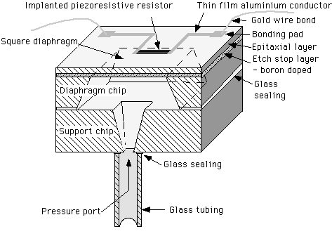
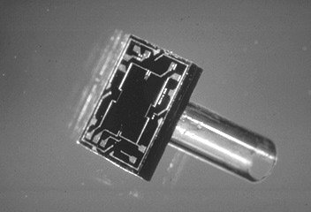
The silicon chip set is shown in Figure 9.1, and consists of diaphragm chip sealed to a support chip which is mounted on top of a glass tubing acting as a mounting stand as well as a pressure port.
The size of the chips is 4*4 mm, chip thickness approximately 0.3 mm, the diaphragm area is typical 2*2 mm and the diaphragm thickness is typical 30 micrometers. The diaphragm is manufactured by stripping off the surface oxide of the silicon wafer by means photolithographic technique in the areas we want the diaphragm cavity. Then the wafer is etched in an anisotropic etching solution with the remaining oxide as masking film. This etching solution attacks the single crystal silicon with different speed in the different crystal directions. The etch is extremely slow in the <1-1-1> direction, meaning that the etch is stopped towards the (1-1-1) planes. The chip material is (1-0-0) silicon, and this means that the etch cavity is surrounded by four (1-1-1) planes which have an angle of inclination of 54.7 degrees relative to the (1-0-0) surface plane, rendering a cavity with four sloped walls as indicated on Figure 9.1.
In this way we can control the diaphragm area, but we also need a technique to control the thickness of the diaphragm, and in this design this is done by doping the silicon with a high concentration boron stopping layer. The etching speed is slowed considerately with increased boron concentration, thereby making it possible to remove the wafer from the etching solution when the slow-etching mode is reached and a well-defined diaphragm thickness is obtained.

Fig. 9.1: Cross-sectioned view of the silicon chip set of the SP80 Pressure Sensor.
However, the process for the ion-implanted piezoresistors is not possible in the boron-doped stopping layer, therefore an additional layer of single crystal silicon has been deposited by epitaxial technique at an earlier stage of the processing. The thickness of the epitaxial layer can be tailored with great accuracy, and together with the stopping layer this gives the total thickness of the diaphragm. The sensing electronics including the piezoresistors is processed on top of the epitaxial layer. This is done by standard techniques well known from the silicon integrated circuit processing technology. The piezoresistors are located along the edges of the diaphragm midway between the corners. This is where we have maximum diaphragm stress due to applied pressure, and by orienting two of them with current direction parallel with the edges and two of them transversal to the edges, two and two will change value with opposite sign as a function of applied pressure. In this way we get a full Wheatstone bridge with four active arms, having a full scale output signal at approximately 30 mV/V. The schematic of the device is shown in Figure 9.2.
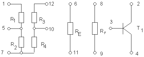
Fig. 9.2: Electrical schematic of the SP80 Pressure Sensor.
The device is mounted and packaged in a transistor header as shown in Figure 9.3. The glass tubing is epoxy sealed to the pressure connection tubing in such a way that the chip set is free-standing on top of the glass tubing and therefore well mechanically and thermally isolated from the transistor header. Mechanical isolation is crucial to obtain isolation from handling and mounting strain, a must to obtain good short-term and long-term stability, and good thermal isolation enhances the temperature accuracy as well as reduces the power requirements when thermostating the device.
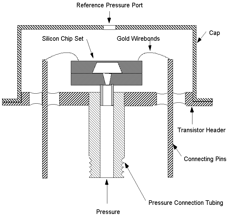
Fig. 9.3:. Cross-sectioned view of the SP80 Pressure Sensor packaged in a transistor header.
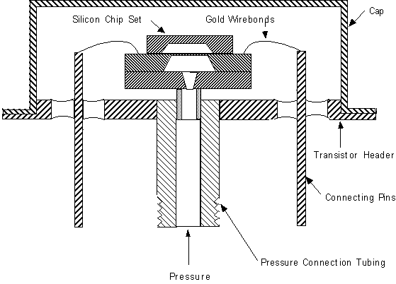
Fig. 9.4: Cross-sectioned view of the SP80 Pressure Sensor with a top chip containing a vacuum reference chamber.
The Reference Pressure Port makes this sensor a differential pressure sensor. If gauge pressure measurement is wanted, the Reference Pressure Port is omitted, and the absolute pressure sensor version has an extra chip sealed on top of the chip set with an etched vacuum reference chamber, as shown in Figure 9.4.
A picture of the assembled unit is given in Figure 9.5, and as can be seen, this sensor is more a system component than a transducer, as electrical connection and interfacing are necessary, as well as mechanical mounting, before the device is ready to measure pressure.
Main features of this sensor are:
Of course, there are drawbacks too:
The bottom line is whether such a device has the preferred price/- performance ratio. At present, this is not always true for micromechanical sensors compared to more traditional sensors or other competing technologies. However, based upon the excellent qualities of silicon as a sensor material combined with its micromachining capabilities and low cost silicon technology batch processing, these sensors are by many believed to be future winners. The main challenge will probably be to come up with sensor designs that combines mechanics, electronics and processing in such a way that high quality, low-priced device are achieved.
 .....
.....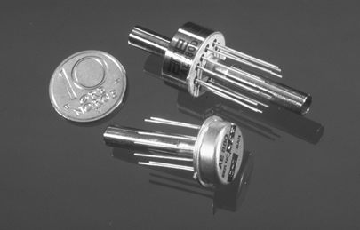
Fig. 9.5: Picture of the SP80 Pressure Sensor.
Rapid advances in silicon planar technology have made micromachined devices competitive
The planar silicon technology has been the busiest workhorse in the advancement and expansion of the integrated circuit technology during the past three decades. This technology is the basis for the modern electronics with all its advanced computers, measurement & control systems, etc. There has been a heavy technology push as well as a strong market pull, the first visualised by Moore`s law saying that the maximum number of components per IC chip doubles approximately every 18 months, and a market growth for the semiconductor industry of about 20% per year. This growth has declined somewhat lately as the industry and market mature, but there still exists strong growth potentials to fuel further technological advances and price/- performance improvements.
Milestones in the planar silicon processing technology:
Micromachined devices are to a large extent based on silicon planar technology because this technology is suitable for these devices, but first of all because these methods are developed to an advanced stage with the strong market pull from the integrated circuit market. This has resulted in a well-assorted choice of advanced processing techniques as well as comparatively inexpensive and diversified processing equipment for manufacturing micromechanical sensors.
Silicon, and first of all single crystal silicon, has been drawing the attention of material researchers in order to push planar silicon processing advances, and therefore silicon is one of the best known materials with both mechanical, chemical and electronic characteristics well known and documented. The low impurity, low-defect single crystal silicon wafers manufactured for the IC industry are, for example, a strong, almost perfect elastic material well suited as spring element in sensors for mechanical quantities.
Based mainly on silicon, the IC world market is more than $60 billions today with still a high growth potential making the IC industry one of the most important industries of the future, not only by its own size, but also because its impact in almost every other industry. An example could be office automation based on electronic information systems built with cheap and powerful silicon integrated silicon chips giving dramatic productivity improvements, or the automobile industry turning from an almost mechanical basis into more and more use of electronics.
The demand for micromachined devices with sensors as area of example
Mainly as a result of the success of the integrated circuit industry, electronic measurement & control systems have become cheap and powerful and gained new markets as technology acceptance has matured.
The central unit of such system with signal conditioning, data processing and communication administration has a record of success, and data presentation systems such as monitors and printers are also reaching an advanced technological level, giving an ever increasing performance increase per $.
These systems need input signals from sensors to handle their tasks, and sensors are more and more becoming the expensive and critical part of such systems because both performance and price have not progressed in the right direction with the same speed. Sensor designs dated back more than two decades are still on the market and competitive, often based on complicated and laborious assembling techniques making them bulky, fragile and expensive.
New sensor designs are often hard to achieve, having to be compatible with harsh environments, rough handling and stringent demands on measuring accuracy, and a lot of consideration, testing and redesign is more the rule than the exception before market acceptance is achieved. This is giving a time lag from idea to running high- volume production that can be several years and sometimes a decade. This time lag severely hampers technological advances within sensor technology, and has also a frightening effect on entrepreneurs, who often prefers to invest their money in less speculative fields with faster investment returns.
This is a tremendous challenge for the sensor industry, and as the market grows and technological advances are made, things are beginning to move with faster speed, and an increasing quality at a declining price is expected in the coming years, though not so dramatic as in the IC industry. Micromechanical sensors are heralded as one of the main roads to achieve these goals in the future as such sensors both have promising high-quality features and can be inexpensively manufactured by silicon batch processing and packaging technology.
Market and applications for micromachined devices with sensors as area of example
Business opportunities for micromechanical sensors have until recently been almost exclusively been in high-tech fields such as medical technology and industrial process control technology. These are fields with long traditions as pioneers in high-tech both from a technological and a funding point of view, fuelling ideas from the university laboratories into manufactured and marketed high-volume products.
These two markets still are the most important with a multitude of applications and increasing number of new business opportunities, but as technology acceptance is achieved, new markets sectors are emerging for micromechanical sensors. The following market sectors with applications examples give an indication on how widespread and diversified the business opportunities for micromechanical sensors are:
· The industrial process control sector market. Application examples:
- Flow sensors in gas pipelines.
- Tank level measurements by pressure measurement.
· The medical sensor market. Application examples:
· The measurement instrumentation market. Application examples:
· The automotive market. Application examples:
· The consumer market. Application examples:
· The agriculture electronics market. Application examples:
· The off-shore oil exploitation market. Application examples:
· The space & military market. Application examples:
Among these markets the automotive market has drawn a lot of attention during the last years as electronics has entered under the hood and into the cabin. The automotive industry has reluctantly started to use more electronics, partly to meet governmental legislation and partly as a result of market pull, and with some and thirty millions cars produced each year, suppliers are tempted with high-volume orders of for instance carburettor manifold absolute pressure sensors. This is the most high-volume application of micromechanical sensors, and it is believed that research efforts and manufacturing facilities set up to produce these sensors will have a major technological impact as well as leading to reduced prices, which again will open up new markets and new applications for micromechanical sensors.
Competing technologies for micromachined devices with sensors as area of example
The competing sensor technologies for micromechanical sensors are multiple and diversified, some based one more traditional hand-crafted technology and some based on modern manufacturing technologies with both general and specific application areas.
Most of them have in common that they are based on old, but fine-tuned technology meaning they are harder to beat than expected from a theoretical evaluation of their advantages and drawbacks compared to silicon micromechanical sensors.
Those sensor technologies that are based on modern manufacturing technologies have almost all just like micromechanical sensors emerged as spin-offs from modern solid state technology and/or general electronics, where large markets have attracted a lot of research efforts.
Among the competing technologies we could mention:
Most often there are four, sometimes two strain gages in each sensor making up the four (two) arms in a Wheatstone bridge. The Wheatstone bridge configuration has several advantages compared to a single gage sensor, among these we would point out better thermal stability, increased linearity and higher sensitivity..Most of today's micromechanical pressure sensors are based on this principle, as the next logical step was to integrate piezoresistive strain gages in a micro- machined pressure-sensitive diaphragm.
To summarise there is a large number of sensor technologies competing on the same or parts of the same market as micromechanical sensors. A rough estimate of the world market for sensors could be $2 billions in 1995, with micromechanical sensor having a market share of some twenty per cent. This market as well as this share is expected to increase in the coming years, but the bottom line is that micromechanical sensors are facing stiff competition from other sensor technologies emphasising the need for improved designs, cost-effective manufacturing and aggressive marketing.
Manufacturers of micromachined devices with sensors as area of example
The industry structure within micromechanical sensors is highly diversified both in size, technological basis and organisation type. Some typical examples can visualise this:
There are of course companies that do not fit into any of these types and some are somewhere in between these types.
Manufacturers of micromechanical sensors are spread all over the world, with USA and especially Silicon Valley as the main location, but also companies in Western Europe and Japan are active as manufacturers of micromechanical sensors. In Table 9.1, several of the manufacturers world-wide are listed.
Since this is a growing field there are many business opportunities and a good guess is that the number of manufacturers will increase in the coming years. Some companies are, according to rumours having problems because they have underestimated the technological difficulties needed to be solved to get market-accepted products, but a shake-out will probably not occur in a long time since the market is growing and a lot of special products with market niches rather than standard products are asked for in the market.
Honeywell |
USA |
Microswitch |
USA |
SenSym |
USA |
IC Sensors |
USA |
Motorola |
USA |
Delco |
USA |
Foxboro/ICT |
USA |
Endevco |
USA |
Kulite |
USA |
Lucas NovaSensors |
USA |
Michigan Microsensors |
USA |
Hitachi |
Japan |
Toshiba |
Japan |
NEC |
Japan |
Yokagawa Hokushin |
Japan |
Toyota Motor Company |
Japan |
Siemens |
Germany |
Philips |
The Netherlands |
Microtel |
The Netherlands |
Xensor Integration |
The Netherlands |
Druck |
UK |
Keller |
Switzerland |
Vaisala |
Finland |
Radi Medical System |
Sweden |
SensoNor |
Norway |
Table 9.1: Examples of manufacturers of micromachined sensors
Research activity in micromachined devices with sensors as area of example
Research activity in this field is very intensive as this a relative new field with the need for a lot more basic research as well as more product and process oriented development to establish a matured technological basis for the involved manufacturers. There is a rather sharp division between scientific research and company research:
· Pioneering research was done and still is done by several universities and research institutions, often sponsored by governmental funding agencies. In Table 9.2 some of the most well known examples are listed. Stanford University in California should be honoured as the pioneer centre, being the first to establish micromechanical sensors as an independent research field, and later several universities and research centres have taken up micromachined sensors as research activity.
Stanford University |
USA |
Case Western Reserve University |
USA |
University of Michigan |
USA |
University of California, Berkeley |
USA |
University of Wisconsin |
USA |
MIT |
USA |
Tohoku University |
Japan |
Kyoto University |
Japan |
Fudan University |
Peoples Republic of China |
Delft University |
The Netherlands |
Twente University |
The Netherlands |
IMEC |
Belgium |
Catholic Un of Leuven |
Belgium |
University of Neuchâtel |
Switzerland |
CSEM |
Switzerland |
Fraunhofer Institute, IFT Munich |
Germany |
Fraunhofer Institute, IMT Berlin |
Germany |
Techn. Un of Berlin |
Germany |
Techn. Un of Denmark |
Denmark |
VTT |
Finland |
Uppsala University |
Sweden |
KTH/IMC |
Sweden |
SINTEF |
Norway |
Table 9.2: Examples of research centres for micromachined sensors
As the technology has matured it has attracted entrepreneurs that have seen its potential for commercial exploitation, and more of the research and development of micromechanical devices have taken place in the laboratories of the manufacturers rather than at the universities. This has lead to a substantial increase of research resources, but also to a less open scientific communication as companies want to keep their acquired technology in secret. However, this field is still characterised by an unusual open scientific communication even from the manufacturing companies, as all parties see the advantage of exchanging their results to fertilise further technological progress. Some processes and designs are patented, but most of these patents are of minor value since technological progress is moving faster than the patent bureaucracy, meaning that the patent often is old- fashioned already before it is properly protected. Therefore, most innovations are not patent protected, but commercial exploited by the innovators simply by keeping it confidential until products are marketed and using the time advantage to make money before the innovation are copied or further developed by competitors.
Research in this field is calling for resources at a lower level than present-day silicon integrated circuit technology, and this has lead to that several centres earlier involved with IC research have taken up micromechanical sensors as their speciality. This has given the field a lot of talented people with academic background in solid state physics using solid state physics in a very successful manner in micromechanical sensor research.
On the other hand, micromechanical sensor research calls for a lot of innovative and competent research related to the field of mechanical engineering, and it looks very obvious that this part has not been given proper attention. This has resulted in a critical need for the micromechanical sensor field to attract talented mechanical engineers to implement state-of-the-art mechanical engineering in new product designs. All in all, research in the field of micromachined devices is a multi-disciplinary research field calling for talents from many fields, and the centres that are able to meet this challenge will probably have a better chance to be successful than others in their research efforts.

Fig. 9.6: A silicon wafer with micromachined diaphragms for condenser microphones made at SINTEF. Batch organised planar processing and micromachining is used to make microphones that have low zero pressure distortion. Controlling the initial mechanical stress by doping the material, 4x4 mm2 diaphragms of thickness 1 micrometer have been made with a resonant frequency of 10-13 kHz for an initial stress of 10-15 MPa. (Photo: Jan D. Martens, SINTEF)
9.2. KEY FACTORS TO SUCCESSFUL INDUSTRIAL INNOVATION OF MICROMACHINED DEVICES
Micromachined device technology is a true-born offspring from integrated circuit technology with silicon as the most used material. Micromachined devices are mostly used as sensors and actuators in microelectronics systems, with sensors being the most important. There are several key success factors specific for micromachined devices are [9.1], [9.2]. We suggest the following subjective list:

Fig. 9.7: The SINTEF/Simrad Optronics Silicon Micromachined Infrared Source as an example of an actuator. This is used in a gas monitoring system , using the absorption of infrared light as sensing principle. Due to the low thermal mass, this actuator can be electrically chopped up to 1 kHz, replacing a bulky electromechanical chopper. (Photo: Jan D. Martens, SINTEF)
|
|
Fig. 9.8. The SINTEF Smart Capacitive Silicon Pressure Sensor, demonstrating the power of combination of features. [9.3] This sensor is using many of the listed features. It has a micromachined diaphragm made by batch processing, as shown in the detail photograph of the diaphragm chip. It uses the variable air gap capacitive sensing principle, has integrated electronics and is assembled by silicon-to-silicon anodic bonding. (Photo: Jan D. Martens, SINTEF)
Micromachined device technology is a part of the microelectronics field. World-wide, microelectronics is recognised as a basic technology commanding the performance and market success of both present and future electronics systems. These are systems that constitute one of the most important key factors determining the effectiveness and competitiveness of most business fields and public administration services. Microelectronics has and will dramatically improve performance both in a revolutionary and an evolutionary way, and this is giving corresponding impacts in those areas using electronics systems based upon microelectronics.
However, the field of micromachined devices is having a much slower development in performance increase, cost improvements and market impact compared to other fields of microelectronics [9.4], [9.5] There are many bottlenecks slowing this development. These trends have motivated us to suggest the following list:
The performance versus cost is a key issue for success in the market for micromachined devices. With competitive performance versus cost ratio, micromachined devices will both replace traditional sensors and open up new applications such as microactuators. Batch processing of micromachined devices used the right way has a strong effect in this respect. At some stage in the production, batch processing is taken over by individual processing such as packaging. The rule of the thumb is that cost per device is very low until individual device processing starts. A good way to visualise this is the price level of commodity integrated circuits, where advanced batch processing technology is driving the cost per transistor into the nano-ECU range [9.4], [9.5],[9.6]. The most aggressively priced micromachined devices such as airbag crash sensors have price targets less than 10 ECU, [9.7], indicating that the batch processing costs are only a few percents of the total production costs.
Extensive and appropriate batch processing methods are very important for successful industrial innovation of micromachined devices. SensoNor, a Norwegian silicon micromachined sensor producer, is focusing on silicon batch processes as their competitive edge. [9.8] They have an annual production of several millions silicon accelerometers used as crash sensors in automotive airbag systems.
Therefore efforts should be made to develop devices that to a larger extent than today is made by batch processing instead of individual device processes. In this review, the most important batch processing technologies appropriate for micromachined devices are presented, together with some examples and recommendations for future work in this area. We have divided these batch processes into 4 groups:
These groups will be described in more detail in the following chapters.
9.3. BATCH PROCESSES ADAPTED FROM MICROELECTRONICS/IC TECHNOLOGY WITH NO OR MINOR MODIFICATIONS
As earlier pointed out, manufacturing methods from microelectronics, primarily developed for silicon integrated circuit manufacturing, are very important cornerstones for the micromachined device technology. They are well developed, commercial processing equipment is available at modest prices, and they have the important feature of batch processing, all ending up in high-quality, cost-effective ways of manufacturing micromachined devices.
We will mention some of these methods and discuss their versatility for micromachined device manufacturing. Their technological fundamentals are rather complex, therefore this overview has to be rather summarising, giving no room for in-depth explanations and analyses. We refer to textbooks [9.9],[9.10] [9.11] for a more comprehensive overview.
Photolithography in IC manufacturing, is the art of photoengraving, which means the process of transferring geometric shapes on a mask to the surface of the semiconductor wafer so that all its surface is protected except where following processes such as etching, implantation or diffusion will take place.
By means of photo artwork a geometric pattern giving the mask openings are transferred from a hand-crafted or computer-aided-designed large-scale layout to the desired pattern on a mask. These steps are most of them very critical calling for high-precision and ultra clean processing until the mask is ready for use. Errors like stepping mismatch or dust contamination must be minimised, as mask errors are copied down on the wafers giving device problems and failures. The mask is usually a right-sized and repeated pattern for use in contact/proximity aligners, or a single enlarged pattern as a reticle that is stepped during registration with a projection aligner.
Pattern is transferred to the wafer by photo registration on the photoresist layer on the wafer that is deposited before registration by spin coated and further processed by selective removal of patterned area. The resulting openings of the developed photoresist are then subject to further processing like etching of the surface oxide or thin film metallisation, and afterwards the remaining hardened photoresist is removed.
A silicon micromachined pressure sensor is an example on how photolithography is used to manufacture micromachined device. Photolithography is used to make an etch opening in the surface oxide for anisotropic etching of the diaphragm.
Spin coating is primarily used for photoresist deposition in photolithography, but has also proved itself as a versatile technique for different polymer and glass coatings, with the material to be deposited spin coated in a low viscosity form, e.g., polyimide in its monomer form imide or glass particles, both in solvents to tailor the appropriate viscosity.
Etching techniques are used in combination with photolithography and other processing techniques to give patterned geometrical and electronic features of the processed device.
Wet etching techniques are mostly based upon organic solutions tailored for photoresist removal and acid or alkali solutions for etching off surface films such as oxides, nitrides and metal films. For photoresist, a selective resist removal of exposed/not exposed photoresist is used, at first to remove the resist in the patterned areas for subsequent processing, then after appropriate processing of patterned areas to strip off the remaining hardened resist from the unpatterned areas. The wet etching techniques of micromachining originated from silicon IC processing.
Dry etching techniques have gained popularity the recent years, both because they for some applications have added features, but also because of cost advantages and environmental issues. Physical etching techniques by sputter etching or ion milling are used to some extent, but combined physical and chemical plasma techniques are most popular. Reactive plasma etching is the most used technique for hardened resist removal. Physical/chemical plasma etching is also much used - e.g., RIE (Reactive Ion Etching) has high flexibility in etching selectivity and is to some extent anisotropic. RIE is extensively used for etching polycrystalline silicon films, e.g., for surface micromachined motor processing.
The thermal diffusion technique as a way of introducing electrical active impurities in a controlled way into silicon is the most important way to alter the electrical characteristics of silicon and other semiconductors. Impurity levels in the range of one/tenth of a percentage and down to parts per million are used to alter the resistivity and type of main conduction mechanism (p-type or n-type) giving the possibility to make resistors, transistors, etc.
Diffusion of impurities takes place in diffusion ovens, operating in the range from approximately 800·C to 1200 ·C with tight temperature regulation and gas as impurity source.
The implantation technique is an alternative way of introducing dopants into a semiconductor. This is done by accelerating the desired impurity ions to high energies and focus them at the semiconductor surface. To cover the whole surface, the ion beam is scanned, and in this way ions enter the semiconductor wafer wherever it is not protected by a mask that can withstand the high energy of the ions. The characteristics of an implantation process are dependent upon type of ionised dopant, ion energy and ion dose per area. The ion energy can be several hundred KeV and the impact creates excessive damage of the substrate material, calling for an annealing step after implantation. This is a heat treatment where the crystal heals itself of the damage and the implanted ions move into substitutional lattice positions and become electrical active.
Ion implantation is often followed by a diffusion step to get the wanted impurity profile going deeper than the few parts of a micron normally achieved by implantation. In this way ion implantation is used as a predeposition technique, using its high dose accuracy to improve the accuracy of the doping. E.g., ion implanted resistors have a resistance value accuracy down to one per cent with excellent matching, and this is many times better than what is achievable with the thermal diffusion technique, and making ion implantation of boron in silicon the dominating way of making piezoresistive micromachined sensors.
SIMOX (Separation by IMplanted OXygen) is a fascinating specialised implantation process applicable for micromachined devices. [9.12] With this technique, a buried dielectric SiO2 layer is made by O2 implantation and subsequent annealing. The dielectric layer can be used for component isolation and/or selective etch stop for micromachined devices.
Epitaxy is used to grow a single crystal (semiconductor) layer of controlled thickness, composition and doping on top of a single crystal (semiconductor) substrate in such a way that the crystal structure of the substrate is extended unperturbed into the epitaxial layer.
Epitaxial growth is done when semiconductor atoms from vapour or liquid phase are deposited on a hot substrate. In order to obtain single crystal growth an almost perfect match of lattice constants is necessary, otherwise polycrystallinity will result.
Silicon-on-silicon epitaxy is used extensively in silicon micromachined device manufacturing. E.g., a selective etch stopping layer for a silicon micromachined pressure sensor is obtained by first doping the substrate with boron at high concentration, then growing an epitaxial silicon layer with phosphorus doping
(n-type) defining the diaphragm thickness and giving a substrate layer for the boron doped piezoresistors. Silicon epitaxy is done in the temperature range from 950·C to 1250·C using for instance silane (SiH4) as vapour source.
Recently molecular beam epitaxy (MBE) has been given much attention from the semiconductor scientific community as a way of making new electronic devices by bombarding a substrate with evaporated material to be deposited. In this way ultra thin single crystal layers with specific doping and electrical characteristics can be tailored. Such structures could also have several applications in micromachined devices, but much basic research needs to be done before this is feasible.
This is a process where vapour phase reaction products are deposited on a substrate as a thin film. Contrary to epitaxial films, these films are either polycrystalline or amorphous. For micromachined devices, two kinds of CVD-films are dominant, either polycrystalline silicon film as piezoresistive element or as surface microstructure in surface micromachining, or silicone nitride film as a masking film for anisotropic and selective etching.
Among the different CVD process techniques Low-Pressure CVD (LPCVD) is known to be the best choice in most cases, with advantages such as precise control of composition and structure, and fast deposition rates.
Plasma enhanced CVD - PECVD allows for lower processing temperatures, e.g., silicon nitride deposition around 300·C for PECVD instead of above 700·C for LPCVD. This gives greater flexibility, e.g., deposition after metallisation, with increased pinhole density as the main penalty.
Thin film technology, or physical vapour deposition (PVD), is a way to deposit solid material on a substrate by vaporising in a vacuum chamber a target material to be deposited by heating (evaporation) or ion bombardment (sputtering) The substrates, when placed in the irradiation field of the vaporised material, will be covered by a uniform polycrystalline or amorphous film of the target material.
In micromachined device processing, PVD is extensively used to deposit dielectric films such as SiO2 for surface passivation, or deposit metals such as aluminium or gold as electronic interconnection conductors and bonding pads.
Resistive films such as tantalum nitride or chromium-nickel can be used when manufacturing micromachined devices by placing thin film trimming resistors on the chip. These are trimmed by laser to obtain specified performance, e.g., zero balance or normalised sensitivity for micromachined sensors.
One special application of PVD in the micromachined device field is deposition of borosilicate glass ("Pyrex") as a bonding material when two silicon wafers or chips are sealed together.
Thin film hybrid technology is often used in connection with micromachined devices. With this technique, some degree of miniaturised electronics can be achieved without putting it on-chip. With this technology, chips, interconnections between chips and high-accuracy resistors are all placed on a substrate.
Thick film technology is the technique to make interconnections and electronic components such as resistors and capacitors on a ceramic or insulated steel substrate by means of screen printing technique. This is a versatile way of making cheap and miniaturised electronics for micromachined sensors, e.g. used as trimming network.
9.4. BATCH PROCESSES MODIFIED FROM MICROELECTRONICS/IC TECHNOLOGY PROCESSES
In this category, we have batch processes that are modified versions of microelectronics/IC technology batch processes. This classification should be seen as the intermediate between the above mentioned adapted processes and the later mentioned specialised processes. There are in this classification also a multitude of processes in use and/or being developed. We will in highlight some examples.
Many micromachined devices need precisely aligned double-sided patterning during the production process, e.g., silicon piezoresistive micromachined pressure sensors have their resistor network processed on one side of the wafer and the micromachined diaphragm processed from the other side. This calls for methods for precise double sided alignment. Mechanical alignment systems ensuring correct x-y positioning by using the circumference of the substrate or wafer as reference is one way to do it, but infrared see-through-wafer aligners are most popular. These aligner are mostly standard aligners with an infrared camera as add-on equipment. At SINTEF we have a Karl Süss MA56 aligner with infrared camera as add-on equipment, and we achieve a side-to-side alignment precision within a few microns.
Standard wafer handling equipment for IC manufacturing are generally made to use the unpatterned backside as attachment side, e.g., attachment to the chuck in spin coaters - with little or no concern for scratches or unwanted deposits on the backside during the process steps. Wafers with double-sided patterning have no backside, therefore equipment and processes must be modified to ensure that both sides of the wafer are properly handled during processing. Somehow, both sides of the wafers must allow for some areas where chuck attachment, manual handling with tweezers, gripping by equipment handling arms, etc., can be done.
The wafer fusion bonding process [9.13] is mainly targeted for silicon-on-insulator fabrication of junction isolated integrated circuits with radiation hardened circuits and high-temperature circuits as focused applications. Nevertheless, the method is an already well established batch process technology for silicon micromachined devices. Clearly, process modifications are needed to optimise the process for micromachined devices.
Wafer bonding proceeds via two steps: Mating of the precleaned hydrophilic surfaces of two mirror-grade polished silicon wafers at room temperature and subsequent annealing at elevated temperatures. During the room temperature step, the final position of the wafers is fixed by attractive interactions between the hydrophilic surfaces. At elevated temperatures (between 400·C and 1200·C) condensation and oxidation reactions take place at the adjacent SiO2 surfaces, which increases the bond strength at the interface.
The LIGA process, which is based on deep etch X-ray lithography, electroplating, and moulding, allows for fabrication of three-dimensional micro structures with high aspect ratios. [9.14], [9.15], [9.16]. LIGA is an acronym abbreviated from the German words LIthographie, GAlvanoformung, ABformung. Its main feature is the ability to make high-precision moulds for micro structures with high aspect ratio that is then used for high volume moulding production, e.g., for plastic parts. The aspect ratio can be as high as 100, e.g., making a structure with width 3 µm and depth 300 µm. Its main drawback is that a synchrotron as X-ray source is needed during the lithographic process. LIGA-like techniques circumvent this drawback by using photolithographics optimised for high aspect ratio instead of X-ray lithographics. [9.17]
Laser micromachining can be defined as processes using lasers the remove, deposit or weld materials in microscale. Laser micromachining is now available as commercial subcontractor services. [9.18]
9.5. BATCH PROCESSES ADAPTED OR MODIFIED FROM OTHER TECHNOLOGIES THAN MICROELECTRONICS/IC TECHNOLOGY
Batch processing is in widespread use in many industries, and many of these process technologies can be adapted or modified for manufacture of micromachined devices. Below, we have given two examples:
Micro stereo lithography can be defined [9.19] as a way to make a 3-D microstructure by using ultraviolet radiation curing polymer, starting from the construction of 2-D sliced thin planes hardened from liquid by UV radiation, which are added to each other as a sequential process resulting in the final 3-d structure. In practice, this is done with a computer controlled set-up of a UV laser and an XYZ alignment system, focusing the laser in the UV curing liquid where hardening into solid state is wanted.
Micro electro discharge machining can be defined [9.20] as micromachining of structures by erosion of material by means of a controlled electric discharge between an electrode and the material. Aspect ratio can be up to 5, with typical width down towards a few tens of micrometers.
9.6. BATCH PROCESSES MAINLY DEVELOPED FOR MICROMACHINED DEVICES
In this category, we have batch processes that are specialised processes for micromachined devices. These processes were developed mainly for micromachined device processing, even though it is easy to see their principal resemblance with microelectronics/IC technology batch processing methods. Some of them are developed from earlier microelectronics/IC technology batch processing methods, but the main development work has been done by the micromachined devices community. We will here highlight some examples.
Bulk micromachining can be defined as three-dimensional micromachining in a bulk material by means of photolithographic etching techniques. This definition covers most bulk techniques used to make micromachined devices, although in some cases mechanical drilling or other machining methods are used. Bulk micromachining in single crystal silicon based on wet chemical etching is the dominating technique, and the way it is done illustrates the concept of in a very informative way. The most popular materials for bulk micromachining in addition to single crystal silicon are glass, quartz and gallium arsenide.
The etching techniques used in bulk micromachining of silicon are most often wet chemical etching, some isotropic and some anisotropic attacking the different crystal direction with different speed. By impurity doping selective etching can be obtained with etching speed dependent upon doping configuration. The anisotropic etching technique is the dominating, as this method, especially when combined with selective etching behaviour, gives the highest dimensional accuracy and repeatability with an accuracy down towards 1mmeter. High accuracy is crucial as this opens up for miniaturisation giving performance and cost improvements for products based on this technology.
|
..... |
Fig. 9.9: Anisotropic etch cavity in (100) silicon with a square masking film opening oriented in parallel with the direction. Due to the four-fold symmetry of the slow-etching (111) planes, sideways etching is stopped giving a cavity with four sloped side walls. The photography shows such an etched cavity.
Surface micromachining [9.21] can be defined as a set of methods to make three-dimensional surface structures, with deposition of thin films as additive technique and selective etching of the thin films as subtractive technique. The thin film system usually consists of a structural layer on top of a sacrificial layer. The sacrificial layer facilitates highly underetched or free-standing patterns of the structural layer.
In practice, single crystal silicon wafer is the dominant substrate material, while chemical vapour deposited (CVD) polysilicon and silicon nitride are most used as the structural layers making up the three-dimensional surface structures on top of a sacrificial layer of silicon dioxide.
A main advantage of surface micromachining, compared to bulk micromachining, is that it does not need double sided processing of the wafers to make three-dimensional structures.
The main additive deposition techniques are evaporation, sputtering, chemical vapour deposition (CVD), and variants of these. The main subtractive methods are selective wet etching and dry plasma etching. Photolithography is used for pattern definition.
The use of sacrificial layers is an important part of surface micromachining. With these methods, etching of the sacrificial layers underneath non-etched thin film structures can be done. In this way several three-dimensional surface structures can be made, such as cavities, supported microbeams, microstrings, diaphragms, lateral mobile microelements, etc.
Anodic wafer bonding is based upon the anodic bonding sealing process that can be defined as a method of electrostatically bonding two dissimilar materials together to form a strong, hermetic seal that involves little alteration in the shape, size, and dimensions of the members making up the joint. It is a high yield wafer-to-wafer sealing method that makes it possible to obtain hermetic seals. The technique was first developed for silicon-to-glass anodic wafer bonding, and has later been further developed to silicon-to-silicon anodic wafer bonding and silicon-to-thin film anodic wafer bonding.

Fig. 9.10: Schematic view of silicon-to-silicon anodic bonding and silicon-to-glass anodic bonding.
The method is further visualised in the below given example from SINTEF.
9.7. HIGHLIGHT EXAMPLE: SINTEF`S SILICON-TO-SILICON ANODIC WAFER BONDING PROCESS
SINTEF have developed a silicon-to-silicon anodic wafer bonding process with high potential of application within both sensor and actuator applications [9.22], [9.23], [9.24], [9.25], [9.26], [9.27], [9.28]. The method was first implemented on chip level, but was later further developed for wafer bonding, making it a batch process.
By choosing proper materials the bonding adds only a small amount of mechanical stress in the structure. This motivated us to develop a silicon-to-silicon anodic bonding for silicon micromachined pressure sensors.
The method is using a sputtered borosilicate glass as a thin film layer on one of the silicon surfaces. The silicon-to-silicon anodic bonding process is similar to the silicon-to-glass process with a few exceptions. Due to the thinner glass layer, the electric field required to drift the mobile ions in the glass can in general be obtained at a lower voltage. Nevertheless, the sputtered glass film will most often suffer from dielectric breakdown unless a dielectric with better isolation properties is deposited on the wafers before sputtering the glass layer.
Sputtered glass films can be used not only as a sealing material, but also as a combined spacer and sealing material. Pattern definition in the glass is best done by gold masking and etching in HF. To avoid etching of the underlying dielectric and thereby dielectric breakdown during bonding, Si3N4 could be used as dielectric (Figure 9.11).
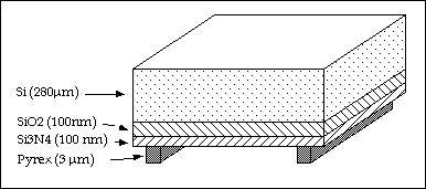
Fig. 9.11: Silicon chip with deposited thin films. The Pyrex is pattern defined by photolitography.
A process with the following parameters is developed:
¥ Sealing wafers together by anodic bonding at approximately 400¡C with an electrostatic voltage of 50 - 200 VDC with the negative electrode connected to the sputter-coated wafer. The voltage should be applied for a time period long enough to allow the current to settle at steady state leakage current to complete the bonding process, typically 10 minutes for a set of 3 inch wafers.
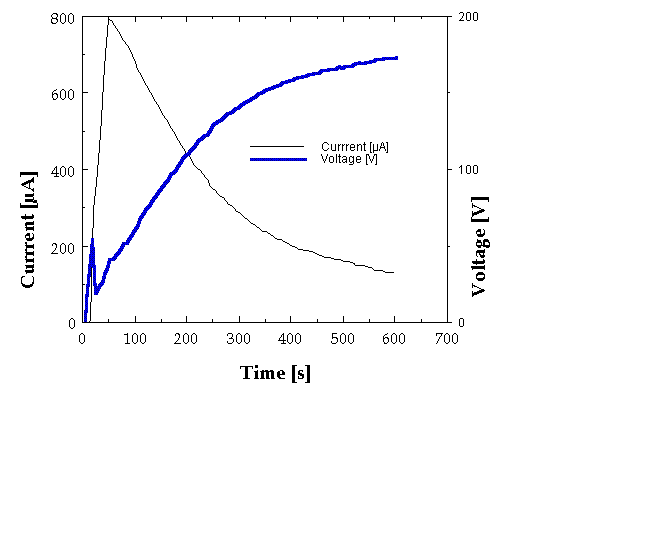
Fig. 9.12 A typical current/voltage versus time relationship during the anodic bonding of two 3 inch wafers.
A typical current/voltage versus time relationship during the anodic bonding of two 3 inch wafers is shown in Figure 9.12.
A crucial parameter for the bonding process is the ratio between bonded and not bonded areas giving the yield of the process. This parameter is dependent of the cleanliness of the wafers and the glass film quality. Poor film quality may cause dielectric breakdown during the bonding process, and unclean areas will not be bonded.
To obtain successful seals, the sealing surfaces should be polished, and utmost care should be taken to avoid particle contamination - proper cleaning procedures and clean room environments (e.g. Class 100) are mandatory to avoid low yield.
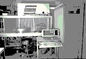
Fig. 9.13: The SensoNor/SINTEF Anodic Bonder. This equipment has a computer controlled bonding chuck for silicon wafers, facilitating flexible set up of bonding temperature and bonding voltage versus time with ramping. The equipment is built inside a flow box to avoid particle contamination. (Photograph courtesy of SensoNor, Horten, Norway)
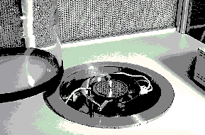
Fig. 9.14: Detail view of the bonding chuck of the SensoNor/SINTEF Anodic Bonder. The chuck is placed inside an air tight chamber to ensure controlled gas environment during bonding, e.g., vacuum or inert gas. (Photograph courtesy of SensoNor, Horten, Norway)
To our knowledge, this batch process is not yet been implemented in full scale commercial use even though the method clearly has advantageous features and has been extensively reported to the international scientific community. This visualises that industrialisation of specialised batch processes for micromachined devices indeed is a difficult task.
9.8. COMPANY PROFILE: SENSONOR IS FOCUSING ON APPLICATION SPECIFIC SENSORS
SensoNor A.S is an independent company operating as an OEM-supplier located in Horten, Norway. The business idea is to develop, manufacture and market microsensors, preferably for high volume applications, based on silicon micromechanics technology. The company has a range of some standard products and offers application specific sensors such for mechanical quantities such as pressure and accelerometers. Over the past 30 years SensoNor has been in the technological forefront to offer microelectromechanical systems (MEMS) solutions to customers. Over these years a broad technological base has been built up. SensoNor has been able to service the demanding task of introducing MEMS solutions to replace traditional sensors in the filed of avionics and precision metrology. Even more so, significant advances have been made in high volume applications such as automotive and medicine. SensoNor is today the world's largest independent manufacturer of crash sensors for automotive applications and a leading supplier of sensors for medical applications.
By 1995 SensoNor employs approximately 300 people, out of which 60 are university graduates including engineers. The company possesses 3 production plants with a total floor space of 8000 square meters. The production lines are built by using a high degree of automation in order to meet customers' expectations for low cost and high reliability. Carefully developed control-plans are utilised to safeguard the production.
SensoNor commits 100% to OEM partners in the challenge to solve application specific need in an optimum way. With a complete authority in both development and manufacturing a focus on the goals with respect to Application Specific Integrated Sensors (ASIS) is given.
Concurrent engineering principles are used in the development of new products. SensoNor's strategy is to complete the development cycle within 2,5 years from the sensor concept is defined until volume shipment takes place. To be able to achieve this goal, parallel exercise of the various engineering disciplines in a given project is a must. This parallel performance is systemised in our engineering approach.
It is of great importance to be self contained when it comes to specialist and tools. The technology group is focused in the core areas of semiconductor processes, 3-D structuring and wafer lamination. A second group is focused in the area of die- and wire-bonding, transfer- and injection-moulding, electroplating as well as trim, form and test. A third group is concentrating on the issues of communicating with the customers and constructing the right type of device for the particular application. As part of the production departments, special engineering groups are focused on specifying and building automatic production lines.
The most advance tools, such as field emission scanning electron microscope, acoustic microscope and chemical element analyses are available to designers and analysts. To be able to optimise designs and to shorten product development time, modelling tools are our daily working environment. They include tools like non-linear FEM and advanced semiconductor process and device modelling. Environmental testing, and "overstressing" play an important role in prototype evaluations. For this purpose there is an in-house laboratory with a range of equipment including combined vibration/temperature testing, autoclaving as well as temperature shock testing.
To further strengthen the engineering position, SensoNor has developed strategic alliances with long term partners within supporting fields, such as basic research, special process development, ASIC design, etc.
SensoNor is self-contained with their own local wafer-FAB and therefore has no need of shopping processing on the market, making the cost structure, delivery security and quality control predictable and reliable. SensoNor has the strategy to develop in house purpose built automatic assembly- and test lines. By doing so, advantage can be taken of applying the right customised packaging concept for a given sensor design. For the purpose of effectiveness in communication there is a short link between engineering support and the production. The company has adopted a Total Quality Management, TQM philosophy, and several quality approvals including ISO 9001 are being granted during 1995.
An example of an application specific integrated sensor from SensoNor is the third generation crash sensor SA30. This accelerometer is optimised to be a low cost crash sensor for airbag systems, with versions for frontal impacts and side impacts. SA30 is a two chip solution with the sensor on one chip and signal conditioning on another chip, packed in a small outline package for surface mount. Mounting on PCB can be normal or horizontal with respect to the sensitive direction. SA30 is completely self-contained with no need for any additional components or trimming.
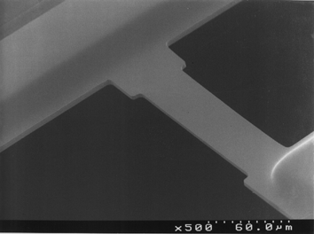
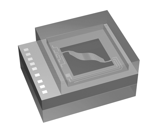
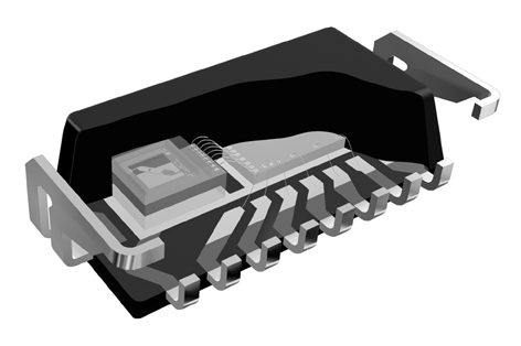
Fig. 9.15: The silicon micromachined resonator beam, the chip set and exploded view of the assembled transfer moulded packaged SA30 Crash Sensor.
The output signal can be either PWM (Pulse-Width-Modulated) for innovative system designs, with respect to noise, EMI or A/D conversion, or analog (ratiometric) for traditional interfacing. A threshold signal is available for designers to improve the system reliability and performance. Due to the intrinsic continuous self-test of the sensor, monitoring of a status signal is all that is needed to check the reliability of the sensor signal. This solution makes it possible to check the sensor at all times, even during a crash without interrupts and loss of information. SA30 utilises a small single crystal silicon resonator which shifts its frequency due to change in acceleration. The innovative concept for self-test has been made possible due to the development of a new sensing principle. Since all parts of the resonator (both "springs" and "mass") are in flexure during operation, the consistency of the function can be monitored continuously. For additional information see ref. [9.29]
9.9. SOME GENERAL RECOMMENDATIONS FOR FURTHER WORK WITH BATCH PROCESSES FOR MICROMACHINED DEVICES
· The transition from batch processing to individual device process steps should be done late in the process flow. Individual device process steps should be scrutinised to be replaced by batch processing or modified to batch processing to increase performance and/or reduce costs.
In practice, wafer dicing is a the critical process step; from then cost-effective, high quality batch processing is difficult or impossible. This bottleneck for industrial innovation of micromechanical devices is a main challenge for this industry. The pioneering costs are extensive, but success here will increase the competitive edge of the individual company and the whole industry. This aspect should therefore be given more attention by the scientific community.
· Updated transfer of suitable state-of-the-art batch processing technologies from microelectronics/IC technology to reach competitive performance versus cost ratio. It is important to stress that the development/pioneering costs of these methods will and should as often as possible be taken by players outside the micromachined device industry. In this way advanced, but mature technologies can be put to work with low costs.
Examples of typical candidates in this category are general IC processing technologies such as photolithographics, diffusion techniques and thin film deposition techniques. SIMOX is an example of a feasible technology that is questionable to put in this category - this technology is clearly driven by IC industry for SOI circuits, but major modifications might be needed for micromachined device applications.
· Development of general batch processing technologies for micromachined devices not readily available from the microelectronics industry that are easy to re-engineer by competitors. The main justification of these methods is to increase the competitiveness of the whole industry, and generally, the costs of such developments are very high. We recommend therefore that these technologies mostly are developed as collaborations in the industry, e.g., collaborative projects sponsored by EU.
Examples of typical candidates in this category are micromachining processing methods and wafer-to-wafer bonding techniques.
· Development of specialised batch processing technologies for micromachined devices that are product specific and difficult to copy by re-engineering. These methods are critical to give the company a competitive edge in the market. We recommend that such processes are aggressively sought for, carefully scrutinised to assure the development costs are justified and can be financed, and carefully protected by stringent confidentiality measures and/or legal actions such as patenting.
Examples of typical candidates in this category are product designs and individual specialised process steps tailored to improve the performance or reduce the cost of the specific product, e.g. replacing individual device filling of silicone oil for vibration damping with batch-processable air damping systems in micromachined accelerometers.
· New designs should be made as simple as possible from a manufacturing point of view. This means that the numbers of needed processing steps are minimised and allowed process variations are generous. In this way efficient, high yield fabrication can be made at low cost. Designs should be based upon design rules established to facilitate such production, instead of first doing a design optimised for technical features and then establish the needed manufacturing processes.
A lot of fascinating micromechanical devices have been developed and reported. However, very few have succeeded as industrial innovations. One important reason is their very sophisticated designs calling for very complex manufacturing technology. Some smart sensor designs are clearly in this category even though they in principle are extensively based upon batch processing. Often, a hybrid approach is much better from a commercial point of view.
· Improved batch organised packaging technologies should be developed.
The main costs for micromachined devices are generally packaging, mainly since batch organised processing at this stage is difficult or impossible. The needed micro assembly techniques are in general rather immature, giving high cost and poor reliability. New techniques need to be developed, adapted or improved by multidisciplinary teams able to handle the different aspects of packaging technology for micromachined devices.
This overview shows that the field of micromachined devices is a very strong and growing industrial fields with a strong market pull from a multitude of applications in different fields and a strong technology push from advanced production technologies, with batch organised process technologies, mainly adapted or modified from corresponding technologies used for silicon integrated circuits. in addition, some specialised processes have been developed for the field.
Batch processing is a key success factor to increase the performance and reduce the costs of micromachined devices. Appropriate batch processes should therefore be used to a larger extent than today to avoid the high cost of individual processing. New devices should be designed and existing devices modified to fulfil this goal. Excellent and suitable batch processes can and should be transferred with no or minor modifications at relative low cost from microelectronics/IC technology. There is an increased use of specialised batch processes for micromachined devices, with micromachining etching processes and wafer-to-wafer bonding as distinct examples. The micromachined device industry should collaborate on the development of generic batch processes to increase the competitiveness of the whole industry, while each company should strengthen their individual competitive edge by developing and implement critical product-specific batch processes.
[9.1] Per Ohlckers & al: "State of the Art of Silicon Sensor Technology" Proceedings of the 2nd Nordic Space Science Technology Workshop. Storefjell, Norway. Oslo, November 23-25, 1992.
[9.2] S. Middelhoek: "Quo vadis silicon sensors?" Sensors & Actuators, 8, 1985, pp. 39-48.
[9.3] A. Hanneborg, T.E. Hansen, P.A. Ohlckers, E. Carlson, B. Dahl and O. Holwech: "An Integrated Capacitive pressure Sensor with Frequency-modulated Output" Sensors and Actuators, 9 (1986) pp. 345-351.
[9.4] S. Middelhoek and A. C. Hoogerwerf: "Smart Sensors : When and Where" Sensors & Actuators A, 41-42, 1994, pp. 1-8.
[9.5] J. E. Brignell: "Quo vadis smart sensors?" Sensors & Actuators A, 37-38, 1993, pp. 6-8.
[9.6] Wojciech Maly: "Growth of Silicon Cost and Resulting Changes in Manufacturing Paradigms", Semiconductor International, No. 6, June 1994, pp. 158-164.
[9.7] Frank Goodenough: "Airbags Boom when IC Accelerometer Sees 50 g" Electronic Design, Volume 39, No. 15, August 8, 1991, pp.45-56.
[9.8] "Micromachined Sensors. The European Source" Brochure from SensoNor, May 1991.
[9.9] Gary E. McGuire (editor): "Semiconductor Materials and Process Technology Handbook" Noyes publications, New Jersey, USA, 1988. ISBN 0-8155-1150-7.
[9.10] R. A. Levy (editor): "Microelectronic Materials and Processes" NATO ASI Series E: Applied Sciences - Vol. 164. Kluwer Academic Publishers, Dordrecht, The Netherlands, 1989. ISBN 0-7923-0147-1.
[9.11] S. M. Sze (editor): "VLSI Technology" McGraw-Hill Book Company, New York, USA, 1983. ISBN 0-07-062686-3.
[9.12] B. Diem, R. Truche, S. Viollet-Boson and G. Delapierre: "SIMOX (Separation by Ion Implantation of Oxygen): A Technology for High-temperature Silicon Sensors" Sensors & Actuators A 21-23, 1990, pp. 1003-1006.
[9.13] Christine Harendt, Wolfgang Appel, Heinz-Gerd Graf, Bernd Höfflinger and Elizabeth Penteker: "Wafer fusion bonding and its application to silicon-on-insulator fabrication", Journal of Micromechanical Engineering, 1 (1991) pp. 145-151.
[9.14] E. W. Becker, W. Ehrfeld, P. Hagmann, A. Maner, D. Munchmeyer: Fabrication of microstructures with high aspect ratio and great structural heights by synchrotron radiation, lithography, galvanoforming and plastic molding (LIGA Process)" Microelectron Eng. 4, 1986, pp. 35-56.
[9.15] W.K. Schomburg, D. Maas, W. Bacher, B. Büstgens, J. Fahrenberg, W. Menz, D. Seidel: "Assembly for Micromechanics and LIGA" Workshop Digest, Micro Mechanics Europe 1994, Pisa, Italy, September 5-6, 1994. pp. 17-27.
[9.16] P. Dario, M.C. Carrozza, N. Croce, M.C. Montesi, M. Cocco: "Non-traditional Technologies for Microfabrication" Workshop Digest, Micro Mechanics Europe 1994, Pisa, Italy, September 5-6, 1994. pp. 86-98.
[9.17] J. Gobet, F. Cardot, F. Rudolf: "Electrodeposition of 3D microstructures on silicon", Journal of Micromechanical Engineering, 3 (1993) pp. 123-130.
[9.18] Advertisement from Resonetics in Solid State Technology, Volume 37, No.5, May 1994, page 7.
[9.19] K. Ikuta, K. Hirowatari: "Real three dimensional micro fabrication using stereo lithography and metal moulding" Proceedings of MEMS 1994, Kanagawa, Japan, January 25-28, 1994, pp. 1-6.
[9.20] T. Masaki, K. Kawata, T. Masuzawa: Micro electro-discharge machining and its applications" Proc. of MEMS 1990, Napa Valley, California, USA, February 11-14, 1990, pp. 21-26.
[9.21] C. Linder, L. Paratte, M.-A. Grétillat, V.P. Jaecklin and N. F. de Rooij: "Surface Micromachining" Proceedings of the MICROMECHANICS EUROPE 1992, Leuven, Belgium, June 1-2, 1992.
[9.22] A. Hanneborg and P. Ohlckers: "Silicon-to-Silicon Bonding Using Sputtered Borosilicate Glass" Proceedings, MICRO MECHANICS EUROPE 1990, Berlin, 26-27 Nov. 1990.
[9.23] Anders Hanneborg, Martin Nese and Per Ohlckers: "Silicon-to-Silicon Anodic Bonding " Journal of Micromechanical Engineering, 1 (1991) pp. 139-144.
[9.24] Per Ohlckers and Anders Hanneborg: "Silicon-to-Silicon Anodic Bonding " Proc of the 14th Nordic Semiconductor Meeting, Århus, June 1990.
[9.25] Anders Hanneborg: "Silicon Wafer Bonding Techniques for Assembly of Micromechanical Elements" (Invited speaker) Proceedings of the MEMS 1991, Nara, Japan, January 1991.
[9.26] Reidar Holm, Terje Kvisteroy, Henrik Jakobsen, Anders Hanneborg and Per Ohlckers: "Stability and Common Mode Sensitivity of Piezoresistive Silicon Pressure Sensors Made by Different Mounting Methods" Proc. of Transducers ´91, June 1991, San Francisco, USA.
[9.27] A. Hanneborg, M. Nese, H. Jakobsen and R. Holm: "Silicon-to-Thin Film Bonding", Proceedings from MicroMechanics Europe (MME) 1992, Leuven, Belgium, June 1-2, 1992. J. of Micromechanics and Microengineering, 2 (1992), pp. 117-121.
[9.28] Per Ohlckers, Anders Hanneborg and Martin Nese: "Batch Processing for Micromachined Devices" Invited paper, Technical Digest of the MME `94, Micromechanics Europe 1994, Pisa, September 5-6, pp 2-16. Appeared in Journal of Micromechanics and Microengineering 5(1995) pp. 47-56.
[9.29] Data sheet: SA30 Crash Sensor; SensoNor A.S, P.O.Box 196, N-3192 Horten, Norway.
Back to the top of "Electronic Components, Packaging and Production"